RSS feed source: National Science Foundation

The U.S. National Science Foundation has announced a $25.5 million investment to support fundamental research and workforce development aimed at enabling future generations of U.S. manufacturing. This year’s awards will support seven research grants and nine seed projects across 36 institutions and companies through the NSF Future Manufacturing (NSF FM) program.

The NSF FM program focuses on areas such as biomanufacturing, cyber manufacturing and ecomanufacturing, with some efforts exploring intersections with quantum manufacturing. The program emphasizes convergence, bringing together teams from across disciplines to create new, potentially transformative manufacturing capabilities, going far beyond improvements to current manufacturing processes.

“The FM program targets critical technical gaps and lays the foundation for emerging sectors, including technologies that haven’t yet been imagined,” said Brian Stone, performing the duties of the NSF director. “NSF is investing in teams that bring together scientific, engineering and manufacturing expertise to equip the American workforce for leadership in advanced manufacturing.”

This year’s FM awards include:

Seven research grants, each receiving up to $3 million over a four-year period, to support multidisciplinary teams conducting fundamental research to enable new manufacturing capabilities, materials, or systems. Projects span a range of topics, including bioengineering in resource-constrained environments, “recyclofacturing” using artificial intelligence to create products from metal scrap, and using robotics and digital twins for additive manufacturing of multi-material systems.Nine seed grants, each receiving up to $500,000 over

Click this link to continue reading the article on the source website.

RSS feed source: National Science Foundation

Americans spend a lot of time on their screens. The images on those screens are made of pixels — tiny dots that represent a single point of color. Scientists from Penn State, including NSF Graduate Research Fellow Nicholas Trainer, recently discovered a process that can make the images on phones, monitors and TVs even brighter.

The Penn State research shows that light emitted from 2D materials can be changed by embedding a second, very small (80,000 times smaller than the width of a human hair) 2D material inside them, called a nanodot. By controlling the size of the nanodot through a process called quantum confinement, scientists can change the color and frequency of the emitted light.

Credit: Nasim Alem, Penn State University

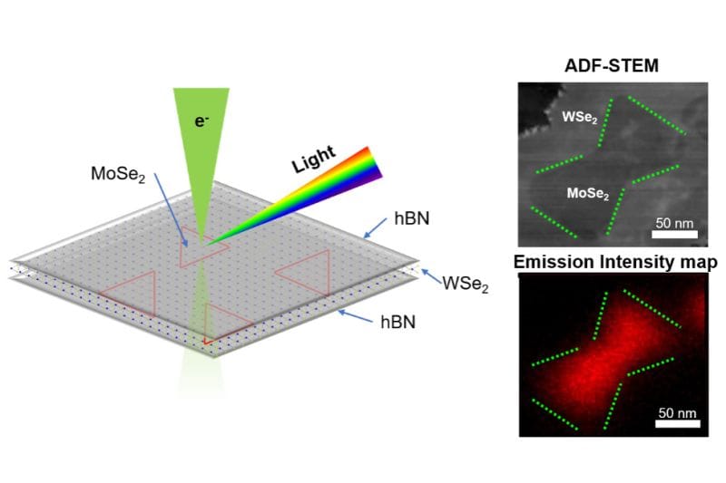
On the left is an illustration of the experimental setup from this study. Molybdenum diselenide nanodots, represented by red triangles, are embedded in tungsten diselenide and encapsulated by hexagonal boron nitride (hBN) on top and bottom. A focused electron beam, shown in green, in a scanning transmission electron microscope (STEM) is aimed at the structure. The emitted light is collected to generate an intensity map. On the upper right is a dark-field STEM image of the molybdenum diselenide nanodot embedded inside tungsten diselenide. The contour of the nanodot is marked by

Click this link to continue reading the article on the source website.
RSS feed source: National Science Foundation

Americans spend a lot of time on their screens. The images on those screens are made of pixels — tiny dots that represent a single point of color. Scientists from Penn State, including NSF Graduate Research Fellow Nicholas Trainer, recently discovered a process that can make the images on phones, monitors and TVs even brighter. Other researchers on the team were also supported by two NSF Faculty Early Career Development awards and used the NSF Materials Innovation Platform at Penn State.

The Penn State research shows that light emitted from 2D materials can be changed by embedding a second, very small (80,000 times smaller than the width of a human hair) 2D material inside them, called a nanodot. By controlling the size of the nanodot through a process called quantum confinement, scientists can change the color and frequency of the emitted light through a process called quantum confinement.

Credit: Nasim Alem, Penn State University

On the left is an illustration of the experimental setup from this study. Molybdenum diselenide nanodots, represented by red triangles, are embedded in tungsten diselenide and encapsulated by hexagonal boron nitride (hBN) on top and bottom. A focused electron beam, shown in green, in a scanning transmission electron microscope (STEM) is aimed at the structure. The emitted light is

Click this link to continue reading the article on the source website.