RSS feed source: National Science Foundation
U.S. National Science Foundation-funded researchers have stabilized a composite material in a superconducting state at ambient or normal, everyday pressure. Their technique, called the “pressure-quench protocol,” offers a new approach for exploring and developing superconducting materials. Superconducting materials have the potential to enable highly efficient electronic devices and minimal energy loss in power grids.
Superconducting materials typically exhibit zero electrical resistance only at very low temperatures or very high pressures, depending on the material. Researchers at the University of Houston overcame these limitations by using their pressure-quench technique to stabilize a composite of bismuth, antimony and tellurium in a superconducting state under ambient pressure. This study, published in Proceedings of the National Academy of Sciences, also included contributions from researchers at the University at Buffalo and the University of Illinois Chicago.
RSS feed source: National Science Foundation
A new chemical process funded by the U.S. National Science Foundation has produced methanol — a type of alcohol essential for manufacturing many common products and a potential fuel source — more efficiently than ever before. The method generates methanol from carbon dioxide nearly 66% more efficiently than the next best approach.
The process uses a dual combination of nickel- and cobalt-based compounds as a catalyst on nanotubes, where multiple chemical reactions and electricity convert carbon dioxide to methanol. More of the C02 is transformed into methanol and with comparatively less electricity consumption, making the overall process more efficient. The findings are published in Nature Nanotechnology by a team of scientists spanning Yale University, Oregon State University and The Ohio State University.
“Methanol is a flexible chemical feedstock that is used for hundreds of common products including plastics, chemicals and solvents,” says Alvin Chang, an OSU doctoral student and coauthor on the study. By improving methanol production, scientists could make it faster, cheaper and with less waste.
Methanol is being explored as a low-cost fuel for generating electricity, powering ships, supplementing gasoline for automobiles and more. In addition to using C02 from the atmosphere, the process could enable methanol production from plentiful agricultural and municipal waste.
Having steady access to such a versatile and renewable resource could transform many aspects of daily life, including the transportation
Click this link to continue reading the article on the source website.
RSS feed source: National Science Foundation
The U.S. National Science Foundation has announced a $25.5 million investment to support fundamental research and workforce development aimed at enabling future generations of U.S. manufacturing. This year’s awards will support seven research grants and nine seed projects across 36 institutions and companies through the NSF Future Manufacturing (NSF FM) program.
The NSF FM program focuses on areas such as biomanufacturing, cyber manufacturing and ecomanufacturing, with some efforts exploring intersections with quantum manufacturing. The program emphasizes convergence, bringing together teams from across disciplines to create new, potentially transformative manufacturing capabilities, going far beyond improvements to current manufacturing processes.
“The FM program targets critical technical gaps and lays the foundation for emerging sectors, including technologies that haven’t yet been imagined,” said Brian Stone, performing the duties of the NSF director. “NSF is investing in teams that bring together scientific, engineering and manufacturing expertise to equip the American workforce for leadership in advanced manufacturing.”
This year’s FM awards include:
Seven research grants, each receiving up to $3 million over a four-year period, to support multidisciplinary teams conducting fundamental research to enable new manufacturing capabilities, materials, or systems. Projects span a range of topics, including bioengineering in resource-constrained environments, “recyclofacturing” using artificial intelligence to create products from metal scrap, and using robotics and digital twins for additive manufacturing of multi-material systems.Nine seed grants, each receiving up to $500,000 over
Click this link to continue reading the article on the source website.
RSS feed source: National Science Foundation
Americans spend a lot of time on their screens. The images on those screens are made of pixels — tiny dots that represent a single point of color. Scientists from Penn State, including NSF Graduate Research Fellow Nicholas Trainer, recently discovered a process that can make the images on phones, monitors and TVs even brighter.
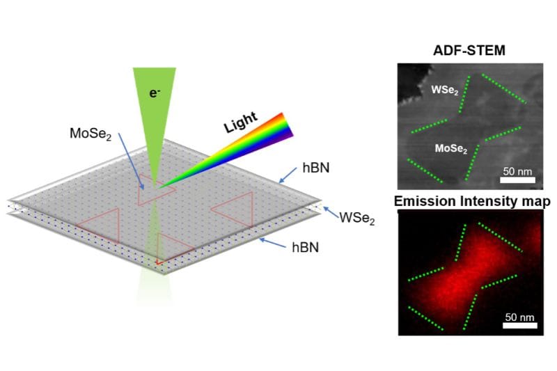
The Penn State research shows that light emitted from 2D materials can be changed by embedding a second, very small (80,000 times smaller than the width of a human hair) 2D material inside them, called a nanodot. By controlling the size of the nanodot through a process called quantum confinement, scientists can change the color and frequency of the emitted light.


